![]()
Please e-mail comments and suggestions for these guidelines and critera.
- III. Clocks
- A. Use of non-low-skew clocks
- B. Chip-to-chip timing strategy
- C. Clock tree
- 1. Use of PLLs and DLLs
- 2. One root for each oscillator
- 3. Show logic blocks and signals crossing clock domains
- 4. Duty cycle analysis for opposite edge clocking
- D. Asynchronous interfaces and failure rate calculations for metastable states.
Clocking, finite state machine design, and timing analysis are all intimately interrelated. This section will discuss some things to check for clocks and design criteria.
A. Use of non-low-skew clocks. Many designers, when first designing with programmable logic, will use "regular" routing resources for clocks, assuming that they are zero-skew paths, such as that found [to a certain extent] on circuit boards using discrete digital microcircuits. However, even though a "net" on a schematic or a clock signal in HDL text appears to be a constant signal, the electrical design of the net must be analyzed. In general, when designers use the non-low-skew resources, the chip may more or less "work" with perhaps some unexplained glitches or a poor "programming yield" that is susceptible to specific routing. So, when sequentially adjacent flip-flops are clock on a common edge, ensure that low-skew clock resources are used. It is acceptable to design with non-low-skew clocks and this can often result in a reduction of power or an effective increase in the number of clocks available. However, careful skew-tolerant design techniques and analysis must be used.
B. Chip-to-Chip Timing Strategy: Many analysis tools are good at analyzing logic within a single chip. However, many are ineffective at analyzing system or chip-to-chip timing. It is tempting to simply use a low-skew clock on a board to hook up various digital devices. However, that is not always guaranteed to work and the proper analysis must be met. In addition to setup time, which is based on a clock period, hold time analysis must be analyzed. This is often overlooked or done improperly. While the worst-case behavior of the clock-to-out of the source chip is easily analyzed using "minimum" or "best case" timing parameters, the hold time of the sink chip must be analyzed assuming a slow path for the clock and the fast path for the data, for the same calculation. Automated tools often do all min or all max but are not capable of doing min-max analysis; often the human must complete this. A good goal for the sink chip is to have a hold time of 0 ns or less (negative hold) but many devices, particularly some models of FPGA, do not satisfy this condition. So, alternate techniques for passing signals must be used, such as opposite edge clocking, treating signals as asynchronous (not preferred), etc. The criteria for passing is that all worst-case setup and hold times are always satisfied or that sufficient metastable state protection is included. Note that some parts marked with a specific speed grade may actually be faster then marked and minimums from the fastest family should be used in the worst-case analysis. Binning criteria for many chips is single ended; a sample timing path is not to exceed some threshold. It is not uncommon for devices that are a speed grade or two faster to be marked as "slower," since device markings are a contractual requirement and devices marked as faster will not be accepted during incoming inspection.
C. Clock Tree
- Use of DLLs and PLLs: DLLs and PLLs can have many useful functions in digital systems. However, they have some requirements that must be satisfied. First check that the worst-case frequencies (both slowest and fastest) are compatible with the circuits; often the acceptable ranges are very limited. Additionally, there are often signal quality conditions that must be satisfied. Next, when these circuits clock finite state machines or other sequential logic, note the time to lock and stabilize for these circuits and ensure that the device and system powers up safely. Another item to check is the worst-case performance when the DLL or PLL is hit by an SEU. This can result in a change of programming of the DLL or PLL, which is sometimes a little subtle, or a change in mode." Safe operation of the system must be ensured during these off-nominal conditions.
- One Root for Each Oscillator: A diagram should be drawn showing the clock trees for the circuit, with one root for each of the oscillators. These diagrams should include PLLs, DLLs, all chips in the clock domain, and all chips that "talk" to the chips in the clock domain. The latter is for the identification of signals that are asynchronous.
- Show Logic Blocks and Signals Crossing Clock Domains: Based on analysis of the clock trees, identify all blocks and signals crossing clock domains and determine the need for metastable state resolution. Additionally, ensure that the latency involved in signal synchronization is tolerable to the system.
- Duty Cycle Analysis for Opposite Edge Clocking: For designs passing data from one edge of a clock to the other, ensure that the worst-case duty cycle for each phase is properly computed. Often designers will assume a 50% duty cycle which is not the case. Sources of duty cycle distortion include oscillator characteristics with 50 +/- 10% duty cycles being common; uneven delays through logic gates and buffers, etc.
D. Asynchronous Interfaces and Failure Rate Calculations for Metastable States: Ensure that proper syncronizers are used for each asynchronous signal. Often designers will simply use two series D flip-flops. While an often used and acceptable topology, for very high-speed circuits for the technology in question the failure rate of this synchronizer is non-negligible; the calculations must be done for these situations. Also note the conditions for which the flip-flop's metastable parameters are taken, with large differences possible in resolution time when moving from nominal temperature and voltage to the extremes. Ensure that there is a lot of margin in these circuits as they are impractical to test and verify. Also note that for ASICs, different flip-flop macros may have significantly different metastable parameters. This can also be a consideration in FPGA. Some discrete devices that are "metastable state hardened" used to be available. Modern flip-flops are pretty good but are not a magical solution.
"Clock Skew" from "Logic Design: Clocking, Timing Analysis, and State Machine Design," presented at the 2002 MAPLD International Conference, Laurel, MD, September 2002.
"Clock Timing and Skew: Real Devices" from "Logic Design: Clocking, Timing Analysis, and State Machine Design," presented at the 2002 MAPLD International Conference, Laurel, MD, September 2002.
Skew-Tolerant Circuit Design, David Harris, Harvey Mudd College © 2001 by Academic Press ISBN 1-55860-636-X.
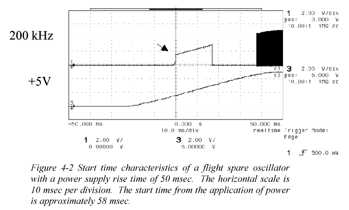
Start times of oscillators may be a function of power supply rise time and may not start up clean. Example with a 50 ms power supply rise time. For the same oscillator, this is a summary of performance over a range of rise times.
"Some Characteristics of Crystal Clock Oscillators During the Turn-On Transient." This application note discusses and shows what the output of an oscillator may be during the turn-on transient. Examples shows include runt pulses of various sizes and polarities.
"Startup Transient," from Advanced Design: Designing for Reliability, 2001 MAPLD International Conference, Laurel, MD, September 10, 2001.
Discussion of MetastableStates
"Clock Skew and Short Paths Timing," Actel Corporation, March 2004.
TOP LEVEL: "Design Guidelines and Criteria for Space Flight Digital Electronics"
Home -
NASA Office of Logic Design
Last Revised:
February 03, 2010
Digital Engineering
Institute
Web Grunt: Richard
Katz